
porcupinetree
not actually a porcupine
- Joined
- Dec 12, 2014
- Messages
- 664
- Gender
- Male
- HSC
- 2015
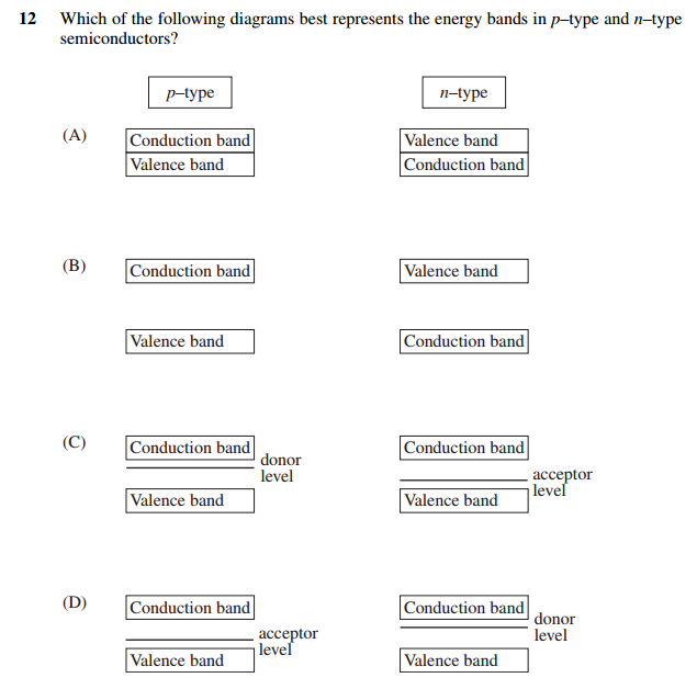
Found this in 2009 HSC. Can someone please explain to me what the terms 'donor level' and 'acceptor level' refer to? I've never heard them before. Thanks
Students helping students, join us in improving Bored of Studies by donating and supporting future students!
TBH, acceptor level isn't what you would normally use to answer P semiconductor question. In these questions they traditionally expect you to talk about the formation of holesThanks guys. Just clarifying: the 'acceptor level' is the amount of energy needed for an electron in silicon (or germanium) to be 'accepted' by the group III element e.g. boron. This amount of energy is much less energy than is required for the same electron to enter the conduction band of silicon. (this explains why p-type doping greatly increases the conductivity of silicon)
Does that sound right?
Yeah ok. Holes is what I would have talked about anyway, given that I wasn't even familiar with the term 'acceptor level' until today. But was my explanation correct?TBH, acceptor level isn't what you would normally use to answer P semiconductor question. In these questions they traditionally expect you to talk about the formation of holes
What you need to say is the following:Thanks guys. Just clarifying: the 'acceptor level' is the amount of energy needed for an electron in silicon (or germanium) to be 'accepted' by the group III element e.g. boron. This amount of energy is much less energy than is required for the same electron to enter the conduction band of silicon. (this explains why p-type doping greatly increases the conductivity of silicon)
Does that sound right?
Yeh. The CSSA 2015 physics trial had a question about p type semi-conductors and their marking criteria had that you needed to mention "aceptor level" so ever since then I always told myself to mention it even if it doesn't necessarily give me a mark.What you need to say is the following:
- Doping with Group III creates an acceptor energy level. This energy level lies just above the valence band and the thermal energy of surroundings is high enough to allow electrons to transition from the VB to the acceptor level. This creates a hole (majority charger carrier) in the VB (electron hole pair), which moves in the opposite direction to electrons in the CB and which enables electrons to flow in the nearly full VB, thus contributing to current.
I actually questioned the guy who is 2IC for HSC Physics marking whether or not acceptor/donor levels need to be known to attain full marks in HSC 2014 Q29.
Question 29 (5 marks)
How does doping affect the way a current is carried in a semiconductor?
Whilst not mentioned in the marking guidelines as such, the notes from the marking centre state this:
Candidates need to improve in these areas
- recognising that doping introduces extra energy levels between the conduction and valence bands (Q.29)
Which to me implies you should mention it if you want to access top marks. He said that he wasn't sure, but I would definitely recommend you mentioning the levels as in order to understand how majority charge carriers are created, you need to understand the transitions between these impurity levels and the VB or CB
Thanks dude, your explanation was really helpful. But with the bit I bolded, wouldn't it be more correct to say that holes move in the opposite direction to electrons in the valence band, given that most electrons which are moving are not located in the conduction band, but are moving within the valence band by 'jumping' into holes?What you need to say is the following:
- Doping with Group III creates an acceptor energy level. This energy level lies just above the valence band and the thermal energy of surroundings is high enough to allow electrons to transition from the VB to the acceptor level. This creates a hole (majority charger carrier) in the VB (electron hole pair), which moves in the opposite direction to electrons in the CB and which enables electrons to flow in the nearly full VB, thus contributing to current.
I get what you are saying, but I have often seen in marking criteria that they want you to explicitly say that holes in VB move in opposite direction to electrons in CB. Ofc electrons in VB move in the same direction as electrons in CB, but they may want you to compare the direction of movement of majority charge carriers. Keep in mind the regular electron-hole pair conduction which is apparent in intrinsic semiconductors I still occurring, the dopant adds an extra mechanism by which conductivity can occur, so there still are plenty of electrons in the CB and they move much more quickly than electrons / holes in the VB also.Thanks dude, your explanation was really helpful. But with the bit I bolded, wouldn't it be more correct to say that holes move in the opposite direction to electrons in the valence band, given that most electrons which are moving are not located in the conduction band, but are moving within the valence band by 'jumping' into holes?